CVD Graphene Films
Showing 13–22 of 22 results
-
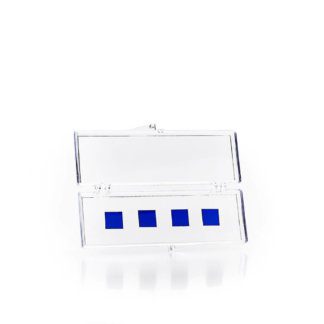
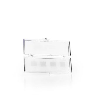
Monolayer Graphene Film Si-SIO2 – 10mm X 10mm
$229.00 Add to cart -
Monolayer Graphene Film-PET-10mm X 10mm
$229.00 Add to cart -
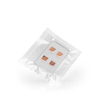
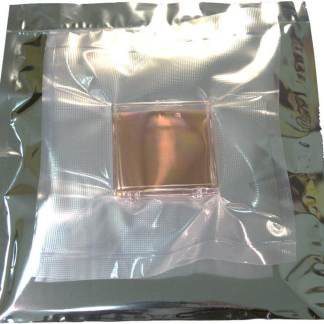
Monolayer Graphene Films on Cu Foil – 10mm X 10mm
$125.00 Add to cart -
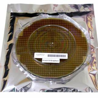
Monolayer Graphene on 6-inch (150mm) Diameter Si/SiO2 Wafer
$650.00 Add to cart -
Monolayer Graphene on 8-inch (200mm) Diameter Si/SiO2 wafer
$950.00 Add to cart -
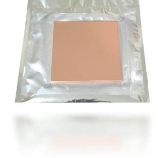
Monolayer Graphene on Copper Foil 3” x 3” (76 mm x 76 mm)
$195.00 Add to cart -
monolayer graphene on copper foil 6” x 6” (150 mm x 150 mm)
$350.00 Add to cart -
Monolayer Graphene on Your Substrate up to 8-inch (200 mm) Diameter Wafer
Read more -
Suspended Monolayer Graphene Films on TEM Grids – 4 pack
$462.00 Add to cart -
Trilayer Graphene Film on Si-SiO2 – 10mm X 10mm
$857.00 Add to cart
What Is Graphene?
CVD Graphene Film Synthesis
Growth Mechanisms
Graphene Transfer
Graphene Structure
Raman Spectra
SEM And Optical Images
Quality Control
Graphene Applications
CVD Graphene Films
CVD Graphene Films are known to have the highest quality, however, the properties of polycrystalline materials are often dominated by the size of their grains and by the atomic structure of their grain boundaries.
These effects are especially pronounced in two-dimensional materials, where even a line defect can divide and disrupt a crystal.
These issues take on practical significance in graphene, a hexagonal two-dimensional crystal of carbon atoms; Single-atom-thick graphene sheets can now be produced by chemical vapor deposition (CVD) on up to meter scales, making their polycrystallinity almost unavoidable.
Theoretically, graphene grain boundaries are predicted to have distinct electronic, magnetic, chemical, and mechanical properties which strongly depend on their atomic arrangement.
Because of the five-order-of-magnitude size difference between grains and the atoms at grain boundaries, few experiments have fully explored the graphene grain structure.
Images reveal an unexpectedly small and intricate patchwork of grains connected by tilt boundaries.
Correlating grain imaging with scanned probe and transport measurements, shows that these grain boundaries dramatically weaken the mechanical strength of graphene membranes, but do not as dramatically alter their electrical properties.
This opens a new window for studies on the structure, properties, and control of grains and grain boundaries in graphene and other two-dimensional materials.
What Is Graphene?
Graphene is a one atom thick sheet or film of carbon atoms. It is strong yet low weight and it conducts heat and electricity. In fact, graphene is the most thermally conductive material known to man.
Scientists had theorized about graphene for decades before it was successfully isolated in the lab in 2004 by Geim et al using scotch tape and graphite.
It is two-dimensional and interacts favorably with light and with other materials. Graphene is a highly crystalline film of hybridized carbon atoms.
Carbon atoms are densely packed in a regular hexagonal sp2 bonded structure. It can best be envisioned as a one-atom thick layer of graphite.
CVD graphene films are the building block for numerous graphene based electronic and photonic devices.
CVD Graphene Film Synthesis
Catalyzed Chemical Vapor Deposition is a process commonly used in carbon nanotube production and integrated circuit manufacturing.
CCVD deposits catalysts onto substrates at high temperatures in a reaction chamber under high vacuum.
As gas vapors condense onto the substrate, a thin film of graphene material is deposited on the surface of the substrate. Temperature is a key parameter to determine the type and morphology of the films produced.
Graphene growth is highly controlled and the films are usually very thin and are made with a very slow deposition rate.
The quality of CVD films combined with the unique properties of graphene have improved the synthesis of graphene a long way from when it was first isolated with scotch tape. CVD films are known for increased hardness, barrier properties, high purity and a fine grain structure.
Growth Mechanisms
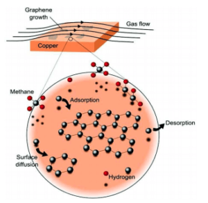
Graphene is grown by catalyzed chemical vapor deposition (CVD) method, depositing graphene films onto the substrate. Typically with a surface coverage of >95% monolayer graphene. Copper is a great growth catalyst due to its low carbon solubility and allows for a self-restricting growth of single layer graphene when compared to other transition metals. Successful graphene growth relies on tuning many variables, including; Copper foil pre-treatment and annealing, growth time, temperatures and pressure, as well as the gas flow rates of hydrocarbon (methane C H4 ), hydrogen and buffer (Argon) gases.
Graphene Transfer
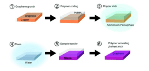
Graphene transfer is available for substrates such as PET that can’t withstand the CVD Graphene Synthesis processing temperatures. The CVD Graphene film can be transferred to other substrates by a variety of methods such as using solvents to release the film from the substrate in a liquid medium and floating it onto a different substrate.
Graphene Structure
A representation of the atomic structure of CVD Graphene Films, note the precise carbon atom arrangement in a monolayer graphene film.The atomic structure of graphene is composed of carbon atoms arranged in six-member rings. Physical properties of graphene depend on the number of atomic layers in the films and the presence of structural defects and impurities.

CVD Graphene Raman Spectra
The raman spectra for our CVD Graphene Films is below.

Graphene Images
An SEM image of our CVD Graphene Films

A TEM image of our CVD Graphene Films

An optical microscope image of our CVD Graphene Films
Quality Control
All our CVD Graphene Films are subjected to a rigorous quality control in order to ensure a high quality and reproducibility of the graphene. CVD graphene films quality control methods are;
Raman Spectroscopy: I(G)/I(2D)<0.5; I(D)/I(G)<0.05
Optical Microscopy inspection of each individual sample to ensure good transfer quality and purity
If your application requires more specific controls (AFM, SEM…) please do not hesitate to contact us.
Graphene Applications
Some of the many CVD Graphene Films applications include Flexible displays, ITO replacement, Graphene research, OLEDs. Researchers continue to find new and innovative graphene film applications.
Showing 13–22 of 22 results