We are always fascinated to learn more about the production processes used fabricate nanoscale products. We grow silver nanowires and have spent significant amounts of time and money developing our process internally. This study reveals previously unknown yet essential ingredients for nanowire growth of germanium nanowires via the vapor–liquid–solid mechanism.
Surface adsorbates are well-established coordinators in material synthesis whose presence has a direct impact on semiconductor nanowire growth. Nanoscale engineering is challenging to say the least and reaction kinetics are critical. Most processes are designed to run right on the line between success and failure. The chemistry – molar ratios, raw materials as well as temperature and pressure are intensely scrutinized and rightfully so but there is an art to it as well. The art is the stuff that you typically don’t find in journal articles or what some consider to be voodoo. This study helps to pierce the veil and will facilitate a greater understanding of reaction kinetics thus giving many researchers greater control of nanowire synthesis thus helping nanoscience push the envelope which hopefully enables further commercial opportunities for germanium nanowires by facilitating a more consistent product with tighter length tolerances. Well done Saujan V. Siveram, Michael Filler, Naechul Shin, Li-Wei Chou et al.
“A study out of GA Tech’s Filler laboratory has gained unprecedented insight into the nanowire growth process through the use of real-time infrared spectroscopy. The study found that surface species, specifically hydrogen atoms and methyl groups, decorate the nanowire’s surface and are essential for the stable growth of nanowires made from germanium.
Without the presence of hydrogen and methyl adsorbing (or adhering) to the nanowire sidewalls, the liquid droplet that sits atop the nanowire could slip, causing growth to cease. “These surface species, hydrogen and methyl molecules, act like a layer of Rain-X, keeping the droplet in place,” Filler explains.
“Our work shows that without these surface adsorbates, growth doesn’t happen. No one knew that before,” says Filler, whose research team published its findings in a recent issue of the Journal of the American Chemical Society. “For as long as scientists have been using this growth method – more than five decades – we didn’t know that anything was present on the wire surface.”
“The fundamental chemical knowledge provided in our study promises to advance the rational synthetic design of nanowire structure and function,” Filler says.
Titled “Direct Observation of Transient Surface Species during Ge Nanowire Growth and Their Influence on Growth Stability,” the study was led by Saujan V. Siveram (PhD 2015) who collaborated with Filler, Naechul Shin (PhD 2013), and Li-Wei Chou, a former postdoctoral researcher at Georgia Tech.”
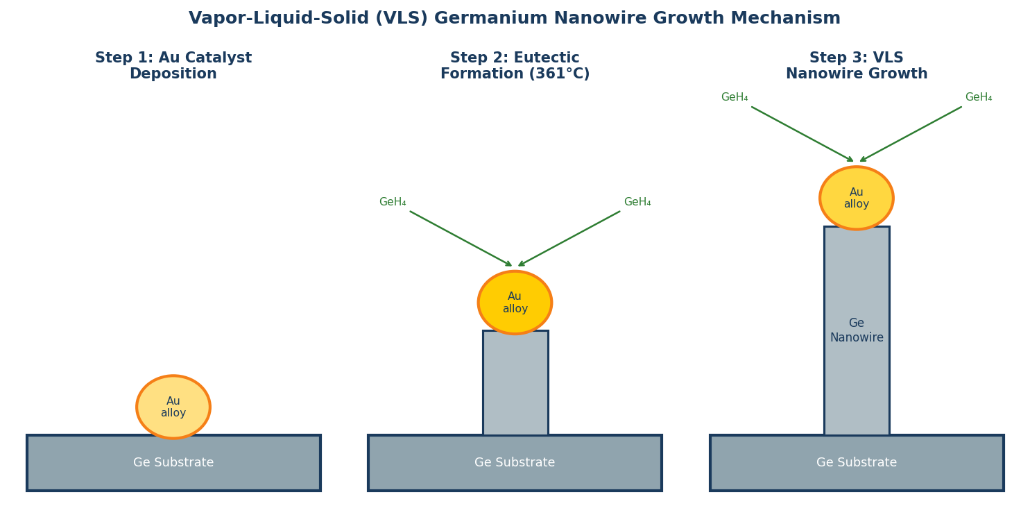
The Vapor-Liquid-Solid Mechanism: A Primer
The vapor-liquid-solid (VLS) mechanism, first described by Wagner and Ellis in 1964, remains the most widely used method for growing semiconductor nanowires with controlled diameter and crystal orientation. In VLS growth, a metal catalyst nanoparticle (most commonly gold) is deposited on a substrate. At the growth temperature, the catalyst forms a liquid eutectic alloy with the semiconductor vapor being supplied. Semiconductor atoms preferentially dissolve into the liquid droplet, supersaturate it, and precipitate out at the droplet-substrate interface as a crystalline solid — pushing the liquid droplet upward and leaving a solid nanowire below.
The diameter of the nanowire is set by the diameter of the catalyst particle. Because catalyst nanoparticles can be deposited with precise size distributions using colloidal methods or electron beam lithography, VLS growth gives researchers control over nanowire diameter from below 10 nm to several hundred nanometers. This is the key advantage of VLS over competing methods such as chemical vapour deposition (CVD) without catalysts or solution-phase synthesis, both of which produce broader diameter distributions.
What the GA Tech Study Reveals: Surface Adsorbates as Hidden Participants
Despite more than five decades of VLS nanowire growth, the detailed surface chemistry at the droplet-wire interface was poorly understood. The assumption in most growth models was that the catalyst droplet and vapor-phase precursor were the only critical participants. The Georgia Tech research upends this assumption by demonstrating that hydrogen and methyl groups adsorbed on the nanowire sidewall are not passive spectators — they are essential for stable droplet retention and continuous growth.
Using real-time infrared spectroscopy — a technique capable of monitoring surface chemistry on the nanowire surface during growth, not just before or after — the team observed directly that H and CH₃ species decorate the sidewall throughout growth. When conditions were changed to remove these adsorbates, the liquid catalyst droplet destabilized and slid off the growing tip, terminating growth. The surface adsorbates act as a wetting layer that pins the droplet to the wire top, maintaining the contact angle required for stable VLS growth.
Michael Filler’s analogy to Rain-X — a surface treatment that helps water bead and run off a windshield by changing the contact angle — is precise: the H and CH₃ adsorbates create a surface energy environment at the droplet-wire contact line that maintains stable wetting. Without them, the contact angle becomes unfavorable and the droplet migrates.
Implications for Nanowire Yield and Diameter Uniformity
The practical importance of this finding is significant for anyone who manufactures or uses semiconductor nanowires. Growth runs that produce a wide distribution of wire lengths — or wires that terminate prematurely — are often attributed to catalyst particle size variation or precursor flow fluctuations. This research adds surface adsorbate concentration as a previously unrecognised variable.
Specifically, the partial pressure of hydrogen and hydrocarbon species in the growth chamber must be maintained above a threshold value throughout the run. Dips in precursor supply, changes in carrier gas composition, or substrate outgassing events can transiently deplete the adsorbate layer, causing droplet instability. Understanding this allows growers to design more stable precursor delivery systems and monitor surface chemistry in real time, dramatically improving run-to-run reproducibility.
For applications requiring nanowires within a tight length tolerance — essential for photonic crystal applications, nanowire solar cells, and field emission arrays — this insight translates directly into higher-value product with less material waste.
Germanium Nanowires: Properties and Applications
Germanium was the semiconductor of choice for this study because its VLS growth chemistry is well-studied and its lower melting point makes the liquid droplet dynamics easier to observe than silicon. Ge nanowires have their own significant application space:
- High-performance transistors — germanium has higher carrier mobility than silicon (both electron and hole mobility), making Ge nanowire FETs attractive for high-frequency and low-power logic applications
- Lithium-ion battery anodes — Ge alloys with lithium at a theoretical capacity of 1600 mAh/g (versus 372 mAh/g for graphite), and nanowire geometries accommodate the volume expansion during lithiation better than bulk Ge particles
- Mid-infrared sensing — Ge is transparent to light in the 2–14 µm mid-infrared range, making Ge nanowires useful as waveguides and sensor elements in molecular fingerprinting applications
- Quantum computing — the strong spin-orbit coupling in Ge and the possibility of inducing p-wave superconductivity in proximity-coupled Ge/superconductor nanowire devices makes them candidates for topological qubits
Carbon Nanowires and CNT-Based Nanowire Composites
While this study focuses on germanium VLS growth, the surface adsorbate principle applies broadly to other nanowire systems grown by VLS or related vapor-solid-solid (VSS) mechanisms — including silicon, gallium nitride, zinc oxide, and indium phosphide nanowires.
Carbon-based one-dimensional materials — single-walled carbon nanotubes and carbon nanowires — occupy a complementary role in the nanomaterials landscape. Where semiconductor nanowires offer tunable bandgap electronics, carbon nanotubes provide exceptional mechanical strength, thermal conductivity, and chirality-dependent electrical properties in structures with similar aspect ratios. Hybrid devices combining CNT interconnects with semiconductor nanowire active elements are an active area of nanoelectronics research.
Cheap Tubes grows silver nanowires in-house, has invested substantially in developing that process, and has supplied research-grade nanowires alongside SWCNTs and MWCNTs to groups around the world. The insights described in the GA Tech paper — about the importance of subtle reaction chemistry variables that don’t appear in standard protocols — mirror our own experience in process development. Nanoscale synthesis is as much craft as chemistry, and understanding the hidden variables is what separates consistent product from variable output.
Sourcing Nanowires and Carbon Nanotube Materials for Research
Cheap Tubes supplies a range of one-dimensional nanomaterials for research groups studying growth mechanisms, device fabrication, and composite applications. Our single-walled carbon nanotubes and nanowires are characterised by TEM, Raman spectroscopy, and SEM for each production lot, with full certificates of analysis. For groups working on nanowire growth process development, we also supply gold catalyst nanoparticles and colloidal dispersions suitable for VLS substrate preparation. Contact our technical team to discuss your specific nanowire or CNT material requirements.
Carbon Nanotube and Nanowire Materials for Research
Cheap Tubes supplies high-purity SWCNTs, MWCNTs, and functionalized CNTs to nanotechnology research groups worldwide. Consistent lot-to-lot quality, full spec sheets, and technical support since 2005.