CVD Graphene Films
Quick Summary: CVD Graphene Films
- What they are — large-area chemical-vapor-deposition graphene grown on or transferred to research-grade substrates
- Why they matter — pristine sp² lattice with macroscopic dimensions for device fabrication, sensing, and microscopy
- Compared to graphene oxide — direct CVD growth, no chemical reduction step, ready for device transfer or growth substrate use
- Key applications — transparent conductive electrodes, field-effect transistors, biosensors, optical microscopy supports, thermal management research
- Available substrates — monolayer on Cu, Si/SiO₂, quartz, PET; bilayer and trilayer films; on TEM grids; transfer-on-request to your substrate
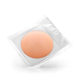
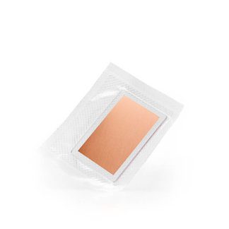
CVD Graphene Films Coated Substrates
Cheap Tubes supplies CVD graphene films on
Cu foil
SiO2/Si
PET or
Quartz substrates
The of CVD Graphene Films are per coated substrate or per 4 pack of coated substrates.
To see the price for a specific product and quantity, please click thru to the individual product page and enter the quantity you need. Our website will display the price for that specific quantity.
Quotes are available online thru our cart. Simply add the products and quantities you need into the cart and then you can print or download a quote.
Available formats include monolayer graphene films on PET substrate, such as the 15mm × 15mm PET-mounted variant for flexible substrate research and bend-test characterization.
Frequently Asked Questions
What substrates is CVD graphene available on?
Standard offerings include monolayer graphene on copper foil (the as-grown substrate), monolayer graphene on Si/SiO₂, on quartz, on PET (flexible substrate), and on TEM grids for microscopy. Bilayer and trilayer films are available for applications that need extra layers without losing the CVD-grown lattice quality. Custom substrates and transfer-on-request to your provided substrate are available.
Can you transfer CVD graphene to my own substrate?
Yes. Send us your substrate (or a substrate spec) and we will perform a wet-transfer or dry-transfer of CVD-grown graphene to it. Transfer adds 5–10 business days to standard lead time. Common transfer requests include unusual rigid substrates, polymer films we do not stock, and pre-patterned substrates with electrodes already deposited.
What is the difference between monolayer, bilayer, and trilayer graphene?
Monolayer graphene is a single atomic layer with the highest carrier mobility and optical transparency (~97.7% per layer). Bilayer graphene has a tunable bandgap when stacked AB and is preferred for FET research. Trilayer graphene shows ABA or ABC stacking variants with distinct electronic properties used in topological and superconductivity research. For most transparent-conductor and biosensor applications, monolayer is the right choice.
How is the graphene quality verified before shipping?
Every batch is characterized by Raman spectroscopy (D, G, and 2D peak ratios) to confirm layer count and defect density. Optical microscopy and SEM imaging confirm coverage and continuity. For monolayer products, the I₂ᵰ/Iᵪ ratio is reported on the Certificate of Analysis along with the D-peak intensity ratio (typically Iᵪ/Iᵪ < 0.1 for high-quality films).
What is the typical lead time?
In-stock items ship in 3–5 business days. Custom transfers and non-standard substrate requests typically take 2–3 weeks depending on substrate availability and characterization requirements. Bulk orders (>50 wafers, >100 cm² cumulative area) are quoted with project-specific lead times.
What documentation ships with each order?
Every order includes a batch-specific Technical Data Sheet (TDS) with substrate, layer count, coverage, and Raman characterization, a current Safety Data Sheet (SDS), and a Certificate of Analysis (COA) on request. Full Raman spectra, optical microscopy images, and SEM images for the specific lot are available for research customers.
Showing 1–12 of 19 results
-
Bilayer Graphene Film Si-SIO2 -10mm X 10mm
$606.00 Add to cart -
CVD Graphene On Si-SiO2 4inch
$1,400.00 Add to cart -
Monolayer Graphene Film on Cu Foil – 1″ X 1″
$115.00 Add to cart -
Monolayer Graphene Film on Cu Foil – 12mm round
$135.00 Add to cart -
Monolayer Graphene Film on Cu Foil – 4″ wafer
$399.00 Add to cart -
Monolayer Graphene Film on Cu Foil – 60mm X 40mm
$325.00 Add to cart -
Monolayer Graphene Film on Quartz – 10mm X 10mm
$275.00 Add to cart -

Monolayer Graphene Film on Quartz 4″ wafer
$849.00 Add to cart -
Monolayer Graphene Film on Si-SIO2 – 4″ round wafer
$849.00 Add to cart -

Monolayer Graphene Film on Si-SiO2- 1″ X 1″
$299.00 Add to cart -
Monolayer Graphene Film PET 1 X 1
$299.00 Add to cart -
Monolayer Graphene Film PET-4
$995.00 Add to cart
What Is Graphene?
CVD Graphene Film Synthesis
Growth Mechanisms
Graphene Transfer
Graphene Structure
Raman Spectra
SEM And Optical Images
Quality Control
Graphene Applications
CVD Graphene Films
CVD Graphene Films are known to have the highest quality, however, the properties of polycrystalline materials are often dominated by the size of their grains and by the atomic structure of their grain boundaries.
These effects are especially pronounced in two-dimensional materials, where even a line defect can divide and disrupt a crystal.
These issues take on practical significance in graphene, a hexagonal two-dimensional crystal of carbon atoms; Single-atom-thick graphene sheets can now be produced by chemical vapor deposition (CVD) on up to meter scales, making their polycrystallinity almost unavoidable.
Theoretically, graphene grain boundaries are predicted to have distinct electronic, magnetic, chemical, and mechanical properties which strongly depend on their atomic arrangement.
Because of the five-order-of-magnitude size difference between grains and the atoms at grain boundaries, few experiments have fully explored the graphene grain structure.
Images reveal an unexpectedly small and intricate patchwork of grains connected by tilt boundaries.
Correlating grain imaging with scanned probe and transport measurements, shows that these grain boundaries dramatically weaken the mechanical strength of graphene membranes, but do not as dramatically alter their electrical properties.
This opens a new window for studies on the structure, properties, and control of grains and grain boundaries in graphene and other two-dimensional materials.
What Is Graphene?
Graphene is a one atom thick sheet or film of carbon atoms. It is strong yet low weight and it conducts heat and electricity. In fact, graphene is the most thermally conductive material known to man.
Scientists had theorized about graphene for decades before it was successfully isolated in the lab in 2004 by Geim et al using scotch tape and graphite.
It is two-dimensional and interacts favorably with light and with other materials. Graphene is a highly crystalline film of hybridized carbon atoms.
Carbon atoms are densely packed in a regular hexagonal sp2 bonded structure. It can best be envisioned as a one-atom thick layer of graphite.
CVD graphene films are the building block for numerous graphene based electronic and photonic devices.
CVD Graphene Film Synthesis
Catalyzed Chemical Vapor Deposition is a process commonly used in carbon nanotube production and integrated circuit manufacturing.
CCVD deposits catalysts onto substrates at high temperatures in a reaction chamber under high vacuum.
As gas vapors condense onto the substrate, a thin film of graphene material is deposited on the surface of the substrate. Temperature is a key parameter to determine the type and morphology of the films produced.
Graphene growth is highly controlled and the films are usually very thin and are made with a very slow deposition rate.
The quality of CVD films combined with the unique properties of graphene have improved the synthesis of graphene a long way from when it was first isolated with scotch tape. CVD films are known for increased hardness, barrier properties, high purity and a fine grain structure.
Growth Mechanisms
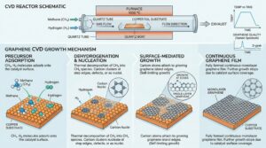
Graphene is grown by catalyzed chemical vapor deposition (CVD) method, depositing graphene films onto the substrate. Typically with a surface coverage of >95% monolayer graphene. Copper is a great growth catalyst due to its low carbon solubility and allows for a self-restricting growth of single layer graphene when compared to other transition metals. Successful graphene growth relies on tuning many variables, including; Copper foil pre-treatment and annealing, growth time, temperatures and pressure, as well as the gas flow rates of hydrocarbon (methane C H4 ), hydrogen and buffer (Argon) gases.
Graphene Transfer
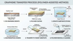
Graphene transfer is available for substrates such as PET that can’t withstand the CVD Graphene Synthesis processing temperatures. The CVD Graphene film can be transferred to other substrates by a variety of methods such as using solvents to release the film from the substrate in a liquid medium and floating it onto a different substrate.
Graphene Structure
A representation of the atomic structure of CVD Graphene Films, note the precise carbon atom arrangement in a monolayer graphene film.The atomic structure of graphene is composed of carbon atoms arranged in six-member rings. Physical properties of graphene depend on the number of atomic layers in the films and the presence of structural defects and impurities.

CVD Graphene Raman Spectra
The raman spectra for our CVD Graphene Films is below.

Graphene Images
An SEM image of our CVD Graphene Films

A TEM image of our CVD Graphene Films

An optical microscope image of our CVD Graphene Films
Quality Control
All our CVD Graphene Films are subjected to a rigorous quality control in order to ensure a high quality and reproducibility of the graphene. CVD graphene films quality control methods are;
Raman Spectroscopy: I(G)/I(2D)<0.5; I(D)/I(G)<0.05
Optical Microscopy inspection of each individual sample to ensure good transfer quality and purity
If your application requires more specific controls (AFM, SEM…) please do not hesitate to contact us.
Graphene Applications
Some of the many CVD Graphene Films applications include Flexible displays, ITO replacement, Graphene research, OLEDs. Researchers continue to find new and innovative graphene film applications.
Showing 1–12 of 19 results