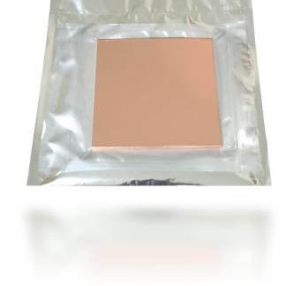
Description
Monolayer Graphene
Transparency: >97%
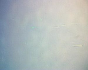
Graphene Coverage: 100% with sporadic adlayers (see optical image above)
FET mobility*: >2700 cm2/(V∙s)
Sheet resistance*: 430 ± 50 Ω/sq
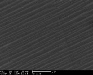
Grain size: >80 um
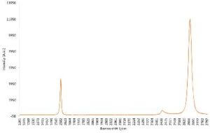
Raman D/G ratio*: Indistinguishable to 0.03
Substrate
Our 8-inch (200mm) Si/SiO2 wafers are sourced from a reliable, quality-assured supplier.
Type/Doping: P/B
Wafer Thickness : 700 – 750 μm
Oxide Thickness: 300 nm
Resistivity: 1 – 25 (ohm-cm)
Orientation: <1-0-0>
Growth Method: CZ
Metal Impurities: 1.00e10 – 5.00e10 (at/cm2)
Raman Spectra
SEM Image
Optical Image