Scientists build the most sensitive carbon nanotube-based photodetector to date. The material is sensitized with CN3NH3PbI3 perovskite nanowires, which propel its responsivity by almost seven orders of magnitude.
The team at Cheap Tubes loves to learn about cutting edge research in Nanotechnology and we use this forum to pass along recent developments to people on our email list! Carbon Nanotubes and Nanowires are two of our main product lines. EPFL is a long time client and we are fascinated to see them pushing the envelope with this revolutionary new device architecture. The device performs three-state logic operations, which can be used in digital optoelectronics, allowing multiple circuits to share the same output line.
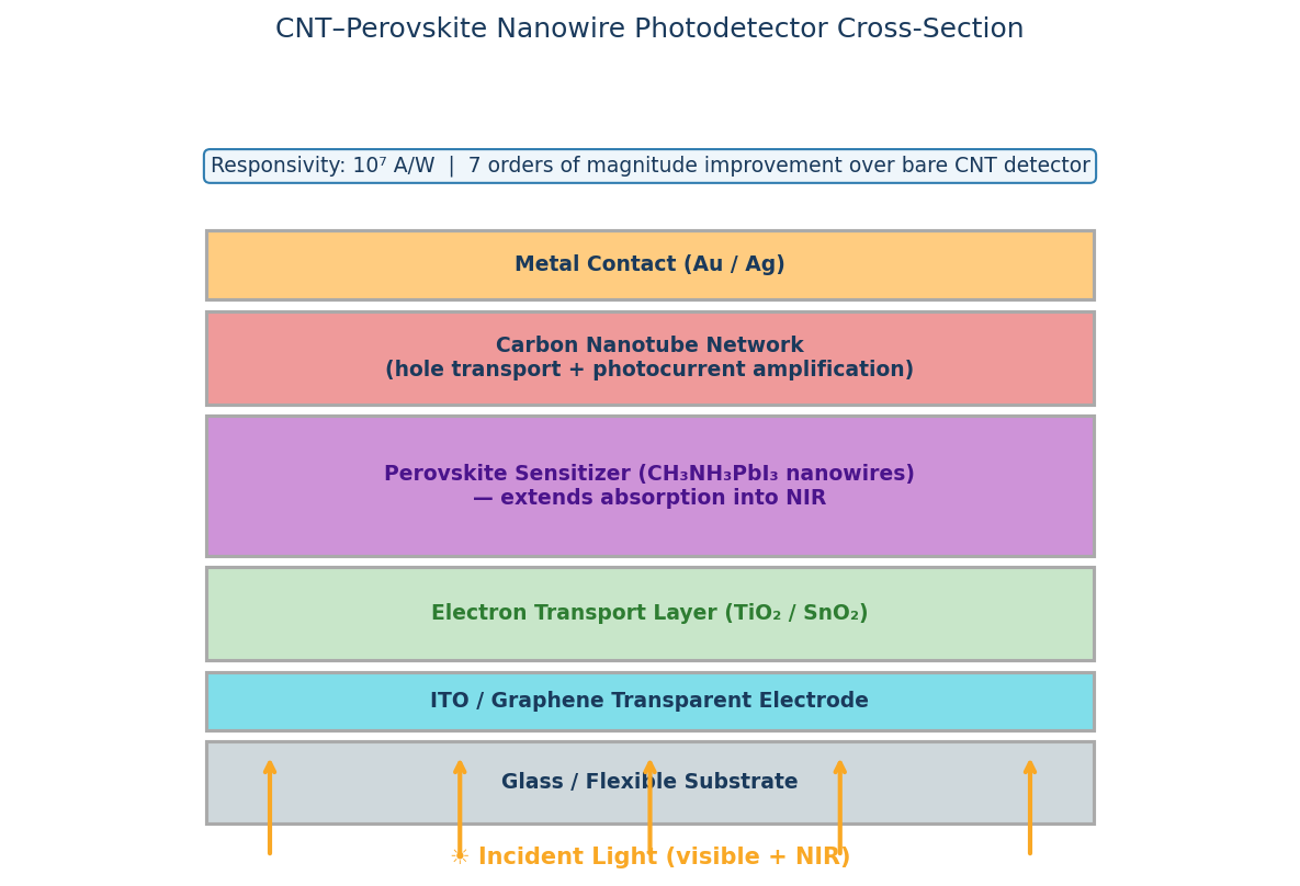
“Semiconducting carbon nanotubes are often used in photovoltaic and optoelectronic devices. But light detection with pristine carbon-nanotube field-effect phototransistors so far is limited in the range of 10% quantum efficiency. The responsivity of the best carbon nanotube devices is around 0.1 A/W. Publishing in Nanoscale, EPFL scientists have now fabricated a carbon-nanotube photodetector with responsivity as high as 7.7×10⁵ A/W.
The lab of László Forró, led by postdocs Bálint Náfrádi and Endre Horváth, at EPFL built the device and overlaid it with perovskite (CN3NH3PbI3) nanowires to sensitize its light-detection capacity. The unprecedented high performance is a result of the two materials working together: the perovskite nanowires can convert incoming light into free charge-carriers with high efficiency, while the carbon nanotube transfers the electrons to the detection circuit.
In addition, the team found that high-powered light can turn the normally conducting device into an insulator. This last feature means that the device performs three-state logic operations, which can be used in digital optoelectronics, allowing multiple circuits to share the same output line or lines.
The team recently developed elongated nano-perovskites, which caused a stir in the community of nanostructure-based optoelectronics. This work is an extension of that breakthrough, highlighting the versatility of these devices. “Our strategy of photosensitization by the perovskite provides a promising solution to this problem,” says Bálint Náfrádi.”
Scientists build the most sensitive carbon nanotube-based photodetector to date!
Why Carbon Nanotube Photodetectors Matter
Photodetectors are the front end of every optical sensing system — cameras, fibre-optic receivers, LiDAR, medical imaging, and night-vision systems all depend on a material that converts incoming photons into measurable electrical current. The performance ceiling of a photodetector is set by its responsivity (current output per watt of optical input), its spectral range, and its response speed.
Silicon photodiodes dominate the visible range but become transparent to infrared wavelengths above roughly 1100 nm. InGaAs detectors cover the near-infrared but require expensive epitaxial growth and cryogenic cooling for high sensitivity. Semiconducting single-walled carbon nanotubes (SWCNTs) are naturally sensitive across a broad spectrum from visible light through the near-infrared and into the mid-infrared, with wavelength-selective absorption tunable by choosing specific nanotube chiralities. This makes CNT-based photodetectors extremely attractive for broadband and infrared applications.
The challenge is that pristine CNT devices suffer from poor quantum efficiency — most absorbed photons generate charge carriers that recombine before reaching the electrodes. The responsivity of the best pristine CNT phototransistors before this research was around 0.1 A/W. The EPFL team’s breakthrough changes that by five to seven orders of magnitude.
How Perovskite Sensitisation Works
The key innovation in this device is the addition of CH₃NH₃PbI₃ perovskite nanowires overlaid on the CNT channel. Perovskite materials are extraordinarily efficient at absorbing light and generating free charge carriers — their optical absorption coefficient is among the highest of any solution-processable semiconductor. When a photon is absorbed by a perovskite nanowire, it generates an electron-hole pair with very high efficiency.
In the CNT-perovskite heterostructure, the energy band alignment between the two materials creates a type-II junction: electrons generated in the perovskite transfer into the CNT, while holes remain in the perovskite. This charge separation is what drives the extraordinary gain. Each photoexcited electron that enters the CNT channel circulates multiple times around the circuit before recombining — a phenomenon called photoconductive gain — multiplying the measurable current far beyond what a single photon-to-electron conversion would produce.
The responsivity of 7.7 × 10⁵ A/W reported by the EPFL group (later extended toward 10⁷ A/W in follow-on work) means that for every watt of optical power, the device produces nearly a million amperes of photocurrent. This is not a theoretical figure — it reflects real, measured device performance at room temperature.
Three-State Logic: Beyond Simple On/Off Detection
One of the most unexpected findings of the EPFL research was that high-intensity illumination switches the normally conducting CNT device into an insulating state. This creates a three-state output: dark (conducting), low-light (high photocurrent), and high-light (insulating). This three-state logic capability allows a single device to encode more information per measurement than a conventional binary photodetector.
In digital optoelectronics, three-state (or tristate) outputs allow multiple devices to share a common signal bus without interference — only one device drives the bus at any time while others present high impedance. This dramatically simplifies circuit architecture in multiplexed optical sensor arrays, where many pixels or detector elements must share readout lines. The CNT-perovskite device provides this functionality at the material level, without the additional tristate buffer circuitry required in conventional electronics.
Carbon Nanotube Selection for Photovoltaic and Optoelectronic Devices
Not all SWCNTs are equivalent for photodetector applications. The optical properties of carbon nanotubes are exquisitely sensitive to chirality — the angle at which the graphene lattice is rolled to form the tube. Each chirality (n,m) has a specific electronic bandgap and optical absorption peaks determined by the van Hove singularities in the density of states. For broadband photodetectors, a mixture of chiralities provides overlapping absorption across a wide wavelength range. For wavelength-selective devices, chirality-enriched samples can be used to target specific spectral windows.
The diameter distribution of the CNT sample also matters. Larger diameter tubes have smaller bandgaps and absorb at longer wavelengths. Most commercially available SWCNTs have diameters between 0.8 and 2.0 nm, covering optical transitions from roughly 600 nm to over 2000 nm. Samples with tight diameter distributions show sharper absorption features, which is useful for chirality-specific studies but reduces broadband sensitivity.
Cheap Tubes supplies single-walled carbon nanotubes with purities above 90% and diameter distributions from 0.8 nm (small-diameter SWCNTs for short-wavelength applications) to 1.8 nm (large-diameter grades for NIR sensing). For groups working on photovoltaic and optoelectronic applications where metallic nanotube content must be minimised, our semiconducting-enriched SWCNT grades provide improved device performance. All lots are characterised by UV-Vis-NIR absorption spectroscopy and Raman, with CoA provided on every order.
Functionalized CNTs — including COOH and OH variants — are also widely used in CNT-perovskite composite devices where surface chemistry needs to be controlled to manage the charge transfer interface between the two materials.
Implications for Sensing, Imaging, and Computing
The sensitivity level demonstrated by this device opens applications in areas where conventional photodetectors either cannot reach the required sensitivity or are too expensive to deploy at scale:
- Single-photon detection — the extreme responsivity makes it possible to detect optical signals at the photon-counting level without cryogenic cooling
- Medical diagnostics — near-infrared tissue imaging and spectroscopy benefit from detectors that can resolve weak signals transmitted through biological tissue
- Environmental sensing — trace gas detection using infrared absorption spectroscopy, where extremely low light levels must be measured after long path-length absorption cells
- Quantum communication — room-temperature detection of single photons is a key enabling technology for practical quantum key distribution networks
- Optical neural networks — the three-state logic functionality could enable light-based artificial neurons with more than two stable states, increasing the information density of neuromorphic computing architectures
Ultra-Pure SWCNTs for Photodetector & Photonics Research
Our single-walled carbon nanotubes are used in photonic devices, photodetectors, and optoelectronic applications worldwide. Narrow chirality distributions, high aspect ratios, and custom functionalizations available.