Description
Monolayer Graphene on Your Substrate up to 8-inch (200 mm) Diameter Wafer
Monolayer Graphene
Transparency: >97%
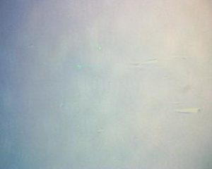
Graphene Coverage: 100% with sporadic adlayers (see optical image above)
FET mobility*: >2700 cm2/(V∙s)
Sheet resistance*: 430 ± 50 Ω/sq
Grain size: >80 um
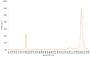
Raman D/G ratio*: Indistinguishable to 0.03
Substrate
Substrates are customer provided and can vary widely. The specific graphene adhesion characteristics cannot be known for all customer substrates; as such, graphene transfer onto custom substrates is conducted on a best-effort basis and results may vary. Please contact us to discuss the properties of the substrate in question.
Raman Spectra
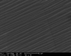
SEM Image
Optical Image